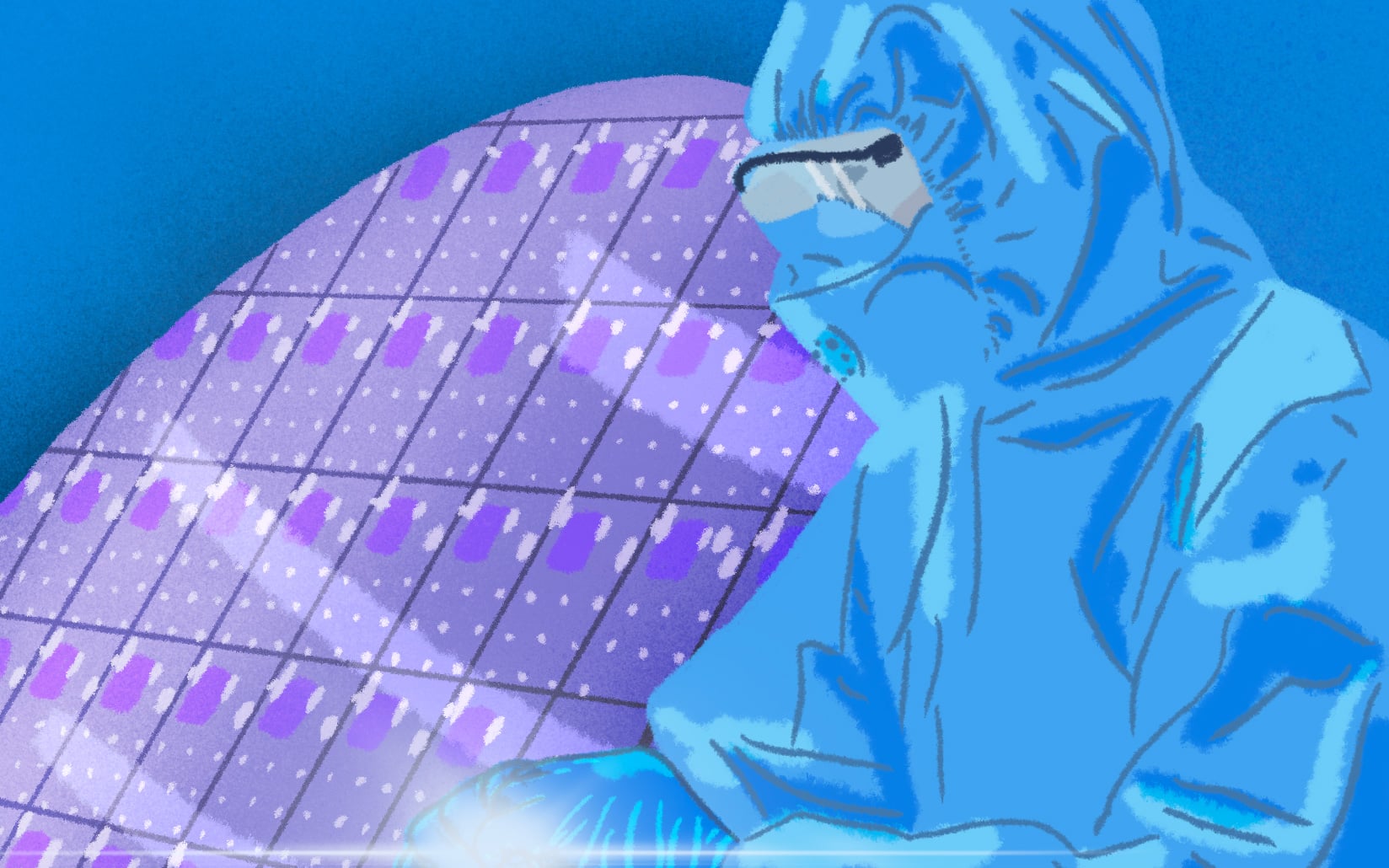
The development and production of energy-efficient electronic components is a major challenge for the microelectronics sector. To answer such a challenge, CEA-Leti and CNRS-LTM does not only focus on building, making and testing new architecture. We also focus on developing greener process and investigating novative solutions to reduce the environmental impact. Precedent works on process step simulation, based on numerical approach, have already been done in CNRS-LTM institute using HPEM tools specialized on plasma etching or at CEA-LETI considering electronic microscope image processing. To be fully operational, these works still need experimental proof. Process characterization could also be another blocking point, whereas the lateral top view dimension could easily be acquire, for example using CDSEM (10 images/mn), the depth and geometry etch profile need complex and time consuming characterization such as TEM (1 image/d). By combining numerical simulation results, physical characterization and fast CDSEM image acquisition technics the PhD student would be able to train a convolutional neural network in order to predict etch profile geometry. These predictions will be helpfully in the future process development and will bring benefits in terms of time to success and financial/environmental cost reduction.