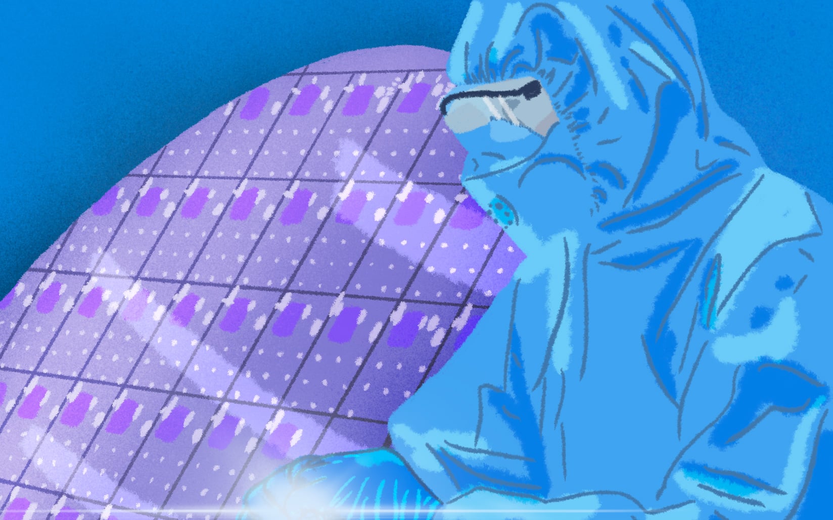
Since 1960, CEA-LETI (laboratory of electronics and information technology) is a driver of French innovation in new technologies domain. Its diverse entities bridge fundamental research and industrial outcomes. One of them, DPFT (department of technological platform) leverages innovation and maturation of new processes for next-generation electronics with its pre-industrial environment grouping together manufacturing and characterization tools. While “standard” printing technologies like photolithography are still developing, CEA-Leti, with various partnerships, explore rupture printing technologies as nanoimprint. This high-resolution printing technic, by mean of a re-usable intermediate mask, could solve dimensional challenge in diverse fields (electronics, optics, photonics, …) with an improved yield (reduction of both cost and time) while offering a more sustainable production method. Nanoimprint could globally reduce process step number but also decrease sacrificial material use thanks to its additive fabrication approach. This new method is an opportunity to review the full integration process, as well as enabling currently impossible integration. However, the limited knowledge of mask replication mechanics on the resist and the potential effects on the following process steps are still a limitation. A numerical model able to handle such question would be very valuable for the development of nanoimprint usage. The final goal of this thesis is to set up a numerical model of mask filling by the resist able to take into account the mask design. In a first step, the model will include the chemical and physical properties of the resist used, as well as the theoretical laws of pattern filling. This model will be evaluated on reference patterns, directly with the tools available in clean room. The key feature of this model is the inclusion of the design, in order to obtain generalizable results. In a second step, the PhD student could change the test patterns to extend the model coverage and/or optimize pattern dimension for a specific end-use. Moreover, the candidate could test influence of different process parameters, as materials or equipment settings, in the clean room facilities. In a general way, the PhD student will have to develop a precise analysis in order to point out the phenomenon in play, potentially construct an experience map but also extend current computing tools on new grounds like 3D patterning. Thesis contract is similar to a fixed-term contract of 3 years, with a gross salary of 2043.54€ the first and second year, and 2104.62€ the final year. Transversal competences developed during this PhD are a great value to continue on high technology domains like nano- and microelectronics or material chemistry, or more generally in any domain with an extensive use of data treatment or physical modelling.
Master 2 / engineering school, materials or nanotechnology