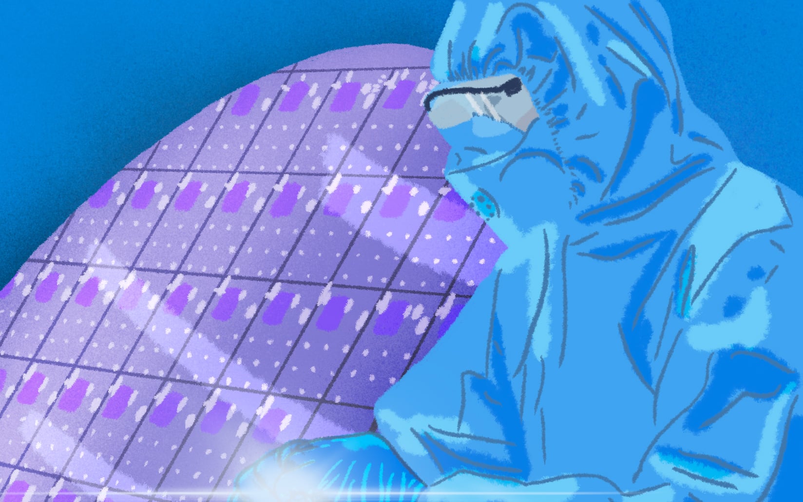
As part of the NextGen project and the European ChipACT to ensure the sovereignty and competitiveness of France and Europe in terms of electronic nano-components, CEA-LETI is launching the design of new FD-SOI chips. Already present daily in the automotive or connected object areas, 28-18nm FD-SOI transistors are produced in large volumes by microelectronics founders such as STMicroelectronics. This technology is based on an innovative architecture allowing the production of transistors that are faster, more reliable, and less energy-consuming than transistors on massive substrates. The move to the 10nm node will improve the performance of this technology while being compatible with the issues of energy efficiency and the challenges of miniaturization. The Field-Effect Transistor (FET) at the 10nm node requires a complex silicon/high-k insulator/metal gate stack. The addition of the high-k dielectric enables to reduce the leakage currents of the gate, but its use coupled with the miniaturization of the components induces new difficulties in the electrical behavior of the FET related to the heterogeneity of the materials constituting the gate stack. To try to resolve these difficulties, this doctorate focuses on an assembly including the deposition of extremely thin metal films on high-k and allowing adjustment of the threshold voltage of the transistors. To study these layers and carry out metallic deposits, CEA-LETI is equipped with PVD equipment for multi-cathode co-sputtering on 300mm silicon wafers. It will make it possible to produce complex alloys and metallic layers adjusted in composition with thickness control at the atomic scale.
Bac +5 avec formation en matériaux/semi-conducteurs