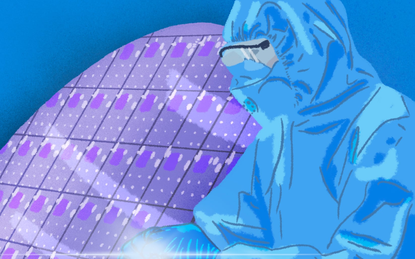
Historically, the development of integrated circuit performance has been based on the reduction in size of individual components. The main driving force behind this miniaturization is photolithography, a key step in the semiconductor component manufacturing process. This process consists in reproducing the design of the circuits to be produced in a photosensitive resin. These complex patterns are generated in a single exposure. Light from an ultra-low-wavelength light source (DeepUV) projects a mask image onto the resin. The higher the optical resolution, the greater the miniaturization of the circuits. When developing new technologies in microelectronics (e.g. FDSOI 10nm, advanced photonics), it is necessary to establish circuit design rules and in parallel to develop photolithography processes to reproduce these designs on the chip. The aim of this thesis is to build bridges between these 2 distinct but closely interwoven worlds, in order to co-optimize their development. Starting from a practical case for advanced technologies, the thesis work will address the following areas/problems: - Improving the accuracy and cycle time of the digital lithography models calibration needed to correct optical proximity effects (OPC); - Using CD-SEM characterizations, identifying borderline design configurations and adjusting design rule constraints accordingly; - Designing innovative patterns that optimize the dimensional space covered, and evaluating them with a rigorous lithography simulation tool and/or experimentally; - Integrating lithography results into design tools to establish causal links with device electrical performance. The thesis will be carried out in Grenoble, at CEA-Leti, internationally recognized for the excellence of its research in the field of microelectronics, and will benefit from the exceptional facilities of the institute's clean room. In particular, the student will be attached to the Laboratoire de PAtterning Computationnel (LPAC), which is exploring ways of improving lithography and etching processes by relying heavily on digital tools, in close partnership with a number of major industrial players. The lab brings together around fifteen people from a wide range of complementary backgrounds (Masters students, student engineers, PhD students, technicians, engineers and researchers, on fixed-term or permanent contracts), who are used to working closely together to give everyone the chance to fulfil their potential and contribute collectively to the progress of the laboratory's work. The student will be expected to publish and share his/her work at various international conferences.