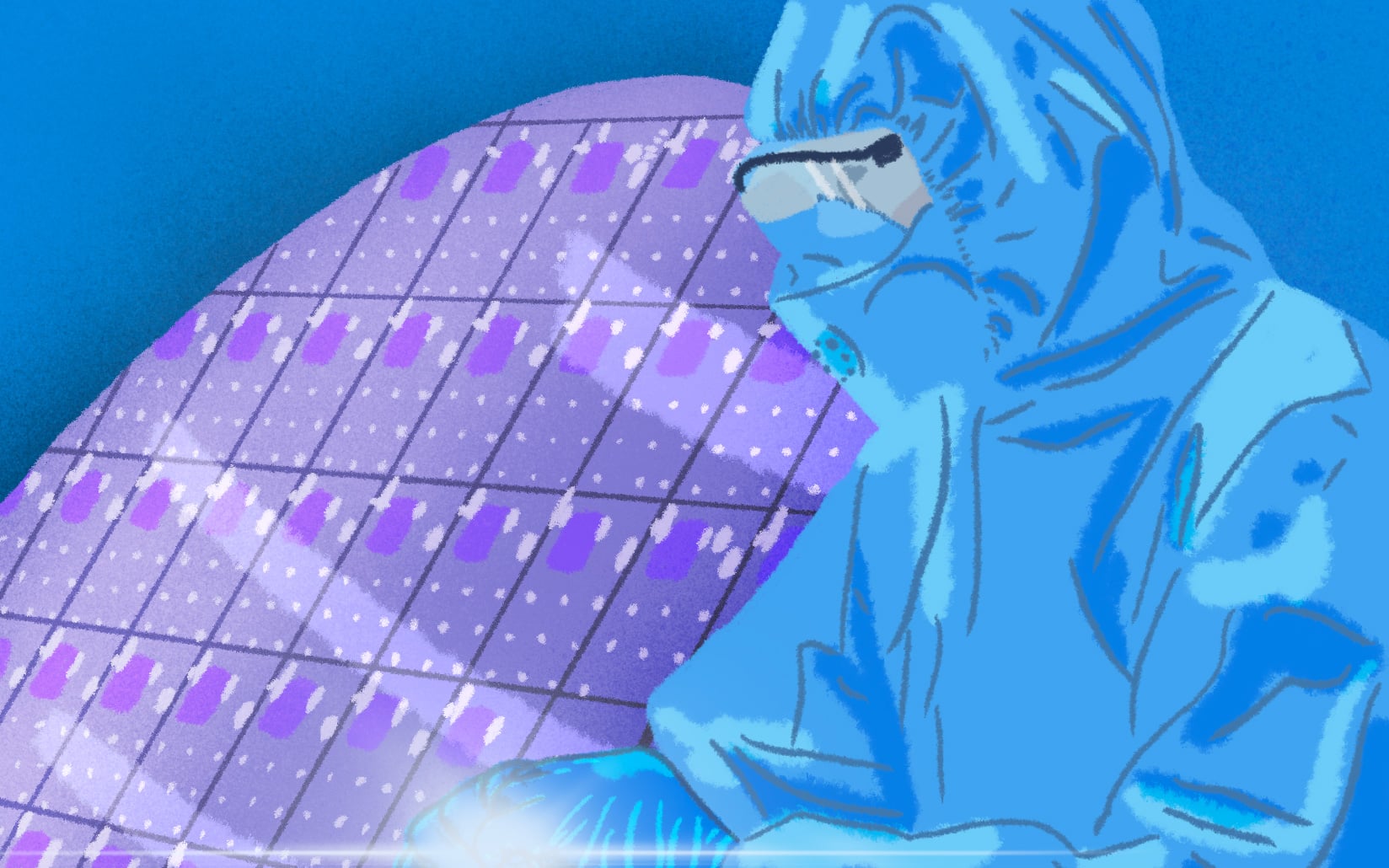
Enhancing the efficiency of energy-conversion devices is a primary goal for numerous international organizations [1]. As a result, the power electronics and wide-band-gap materials industries require significant development effort to align with these objectives. Particularly, recent progress in silicon carbide (SiC) processing technologies [2]–[4] show that innovative substrate architectures have the potential to offer state-of-the art opportunities. These designs can enable us to achieve better performance while simultaneously reducing environmental impacts. With this Ph.D. subject, we propose to explore new frontiers beyond these recent developments. The research objectives of this subject are to develop a clean room process for transferring a thin layer of Ga2O3 layer onto a polycrystalline bulk SiC substrate using the Smart Cut™ technology [5]. This architecture will allow to benefit from the exceptional ultra-wide bandgap and high breakdown electric field of the Ga2O3 material, while compensating for its low thermal conductivity with that of SiC. Numerical simulations will be developed to study the electrical and thermal conduction mechanisms across the Ga2O3/SiC interface. In parallel, the technological manufacturing of double-layer substrates in a clean room will be fine-tuned so as to be able to characterize the electrical and thermal performance of such a heterostructure. Advanced physico-chemical characterizations (TEM, Raman, SIMS, XRD, etc.) will be used to complete the global material study. [1] European Commission, Energy, Climate change, Environment, 2022. [Online]. Available: https://energy.ec.europa.eu/topics/energy-efficiency/energy-efficiency-targets-directive-and-rules_en [2] S. Rouchier et al., Materials Science Forum, vol. 1062, pp. 131–135, 2022, doi: 10.4028/p-mxxdef. [3] O. Bonnin, E. Guiot, and W. Schwarzenbach, Coumpound Semiconductor Issue, vol. 27, no. VI pp. 18-22, 2021. [Online]. Available: https://compoundsemiconductor.net/magazine#y2021 [4] G. Gelineau et al., Materials Science Forum, vol. 1089, pp. 71–79, 2023, doi: 10.4028/p-026sj4. [5] M. Bruel and B. A. Auberton-Hervé, Jpn. J. Appl. Phys., vol. 36, no. 3S, p. 1636, 1997, doi: 10.1143/JJAP.36.1636.