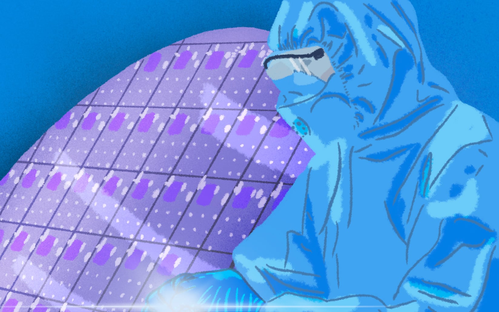
As part of the microelectronics growth plan, driven by the European directive France 2030, CEA Leti is acquiring new state-of-the-art tools and developing new technologies for future applications. The challenge is to develop several technological building blocks enabling the industrial transfer of microelectronic processes down to the 10nm technology node. Lithography is the most critical step in the manufacturing of a component, as it enables the definition of addressed patterns (dimensions, shapes, etc.), which is why R&D work on this step requires particular attention to meet the needs of the industry. Up to now, it was enough to monitor the two key parameters in order to ensure the device performances: - Critical dimension uniformity (CDU) across the wafer - Overlay (OVL), which represents the relative intra-field position of two lithography levels compared to their theoretical position. However, reducing pattern size requires a more global view of these control parameters. In this case, the term “placement error” is well more adapted. It combines CDU and OVL, answering the question: where "trully" is the pattern in relation to its ideal position? Many studies (i.e. Mulkens J., et al. Proc. SPIE 1014505, 2017) have shown a significant dependency relation of placement error with several parameters, such as follow : Optical proximity correction (OPC), registration error (mask related), resists, exposition & development step, overlay, CDU or resist roughness. The placement error budget is therefore becoming very critical in the industry, and is highly correlated with the state-of-the-art capabilities of the equipment to ensure the processes. The aim of this thesis will therefore be to understand the technological issues raised by process integration on placement errors at field and wafer scale. In addition, solutions will be proposed for characterizing intra-field deformation and optimizing intra-field performance in 193 immersion lithography to meet the requirements of sub-10nm technologies. The main axis of this thesis could be described as follow: 1/ To Acquire an understanding of the topic challenges by deep literature monitoring and knowledge of the strategies in place currently in microelectronics. 2/To Get acquianted with cleanroon environnment and to learn working on new generation equipments, specifically on 193i lithography scanner and metrology tools recently installed. Several formations will be displayed. 3/ All over the thesis, to publish (scientific reviews) and share results and achievements on different conferences 4/ Thesis manuscrip writting & presentation This work is integrated into the Lithography laboratory (LLIT) of CEA Leti Silicon plateform division (DPFT). You will be part of a dynamic and multidisciplinary team: from optical photolithography process to alternative lithography such as nanoimprint and ebeam lithography expertise, on state-of-the art clean room equipments. The team works in synergy with industrial partners that allows an efficient transfer of Leti innovations.