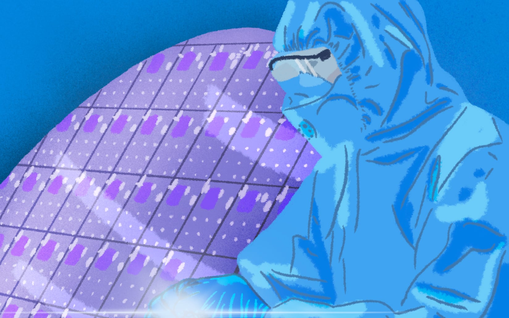
As digital content demand surges, 6G systems face major challenges, particularly in developing power amplifiers for Sub-THz frequencies. These frequencies promise ultra-high data rates but push the limits of current silicon technology. In AI datacenters, optical communication between GPUs is a must to reduce the total energy usage, compared to classical wiring. The highest speed devices are then needed in photodetectors amp; lasers’ electrical drivers. InP-based Heterojunction Bipolar Transistors (HBTs) on large silicon substrates offer a promising solution, combining high-speed performance with minimal system losses. This technology comes with the challenges of integrating III-V layers with CMOS-compatible processes while allowing promising new device architectures, for both electrical parasitics reduction and self-heating management. This PhD program aims to guide Leti’s III-V HBT on Si developments to optimize the device architecture and increase the RF performance. In this program the student will: Perform electrical characterization of various device geometries and technological splits through DC and RF measurements such as IV, thermal analysis, S-parameters and possibly Load-Pull. Simulate key parasitics and new device architectures to understand device limitations Collaborate closely with process engineers to link electrical results with fabrication choices and guide device optimization