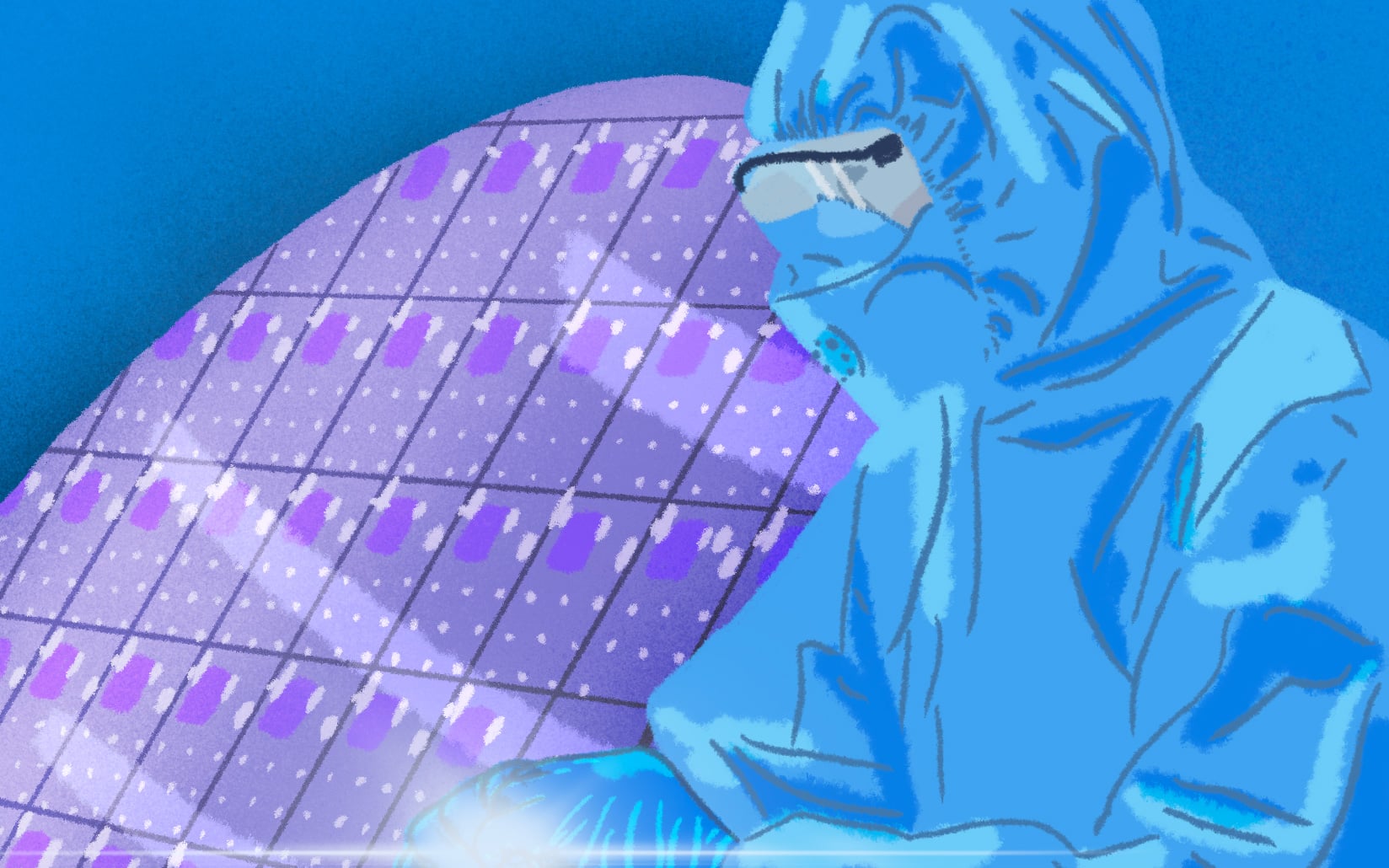
Optoelectronic devices such as CMOS Image Sensors (CIS) require the realization of 3D structures, convex microlenses, in order to focus photons towards the photodiodes defining the pixels. These optical elements are mandatory for the device efficiency. Their shape and dimension are critical for device performances. In the same way, devices based on diffractive optic and hyperspectral sensors are looking for complex multi-height structures. Finally, recent micro-display technologies for augmented reality (AR) and virtual reality (VR) require 3D structures difficult to achieve with conventional micro-fabrication technics. Leti is at the state of the art on an alternative photolithography technics, so-called Grayscale. This process can produce a whole range of 3D structures not available with standard photolithography, such as concave, elliptic, pyramids and asymmetrical shapes. These structures could be used in a large number of application fields, like photonics and micro-displays (AR/VR). Once these structures achieved in photoresist, it is necessary to transfer them in an adapted functional layer using plasma etching. The etch mechanisms behind the transfer of micrometric 3D patterns into a polymer layer have been recently studied at Leti. To address new application needs, it is interesting to transfer these structures into silicon based inorganic layers because of their optical properties. Furthermore, the 3D pattern dimensions, currently few micrometers, need to be sub-micrometric for the most advanced technologies. In these condition, pattern transfer fidelity of 3D structures is even more challenging and it underlines why the etch mechanisms need to be well understood. Currently the transfer into inorganic layers by plasma etching of submicronic 3D patterns obtained with Grayscale photolithography is not well studied in literature. Consequently, this thematic is innovative and has a real benefit. The goal of this PhD thesis is to study and understand the etch mechanisms in order to control the shape and dimension of the transferred structures. The work will be very experimental and will be mainly performed in Leti’s 300mm cleanroom. You will have access to a last generation plasma etch tool and numerous characterization technics. This thesis is in collaboration with the photolithography department and in interaction with different teams, such as the silicon platform and application department.