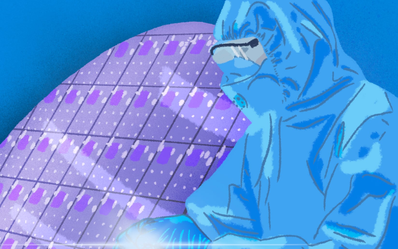
Future microelectronic components will be ever smaller and ever more energy-efficient. To meet this challenge, 2D materials are excellent candidates, thanks to their remarkable dimensions and electronic properties (high mobility of charge carriers, high light emission/absorption). What's more, they feature van der Waals (vdW) surfaces, i.e. no dangling bonds, enabling them to retain their properties even at very small dimensions (down to the monolayer). New 2D materials and vdW stacks with novel physical properties are being discovered every day. However, integrating them and measuring their performance in circuits remains an ongoing challenge, as their properties must be preserved during integration. The aim of this post-doc is to develop components for qualifying 2D materials for microelectronic (RF transistor) and spintronic (magnetic memory) applications in horizontal configuration on silicon. A vertical measurement method has already been developed by CEA LETI. Building on these developments, the candidate will develop this measurement system and characterize various materials produced in MBE by CEA-IRIG. The work will involve transferring these layers onto chips, optimizing the electrical contacts and developing the in-plane electrical measurement chain.